D Flip-Flop or Delay Flip-Flop is the fundamental building block for any sequential circuit. Check out how we can code this in Verilog.
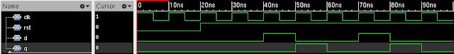
Function of D Flip-Flop: At every clock edge, the output q follows the input d. Meaning that whenever input d changes, it will be obtained by the output q at the next clock edge.
Schematic:

Verilog Code:
Testbench:
Simulation Result:
Note:

Concluding Notes:
Function of D Flip-Flop: At every clock edge, the output q follows the input d. Meaning that whenever input d changes, it will be obtained by the output q at the next clock edge.
Schematic:

Verilog Code:
module DFlipFlop(d,clk,rst,q);
input d, clk, rst;
output q;
reg q;

always @ (posedge clk or negedge rst) // Asynchronous Reset
begin
if(!rst)
q <= 1'b0;
else
q <= d;
end
endmodule
Testbench:
module DFlipFlop_tb;
 reg d;                  // Inputs
 reg clk;
 reg rst;
 wire q;                 // Outputs

// Instantiate the Unit Under Test (UUT)
 DFlipFlop uut (
  .d(d),
  .clk(clk),
  .rst(rst),
  .q(q)
 );

 always #5 clk = ~clk;

 initial begin
  d = 1'b0;          // Initial values
  clk = 1'b0;
  rst = 1'b0;
  #20 rst = 1'b1;

  #20 d = 1'b1;      //Provide values for d
  #10 d = 1'b0;
  #20 d = 1'b1;
  #20 d = 1'b0;
  #50
  $finish;
end
endmodule
 |
| Click on image for better view |
Note:
- In the testbench, do not change the d input exactly at a clock posedge. The simulator will capture the output q at that posedge itself and the simulation will be wrong (depending on the simulation tool).
- Also it will lead to violation of setup/hold times of the flip-flop (However, simulator tools consider zero setup/hold times).
Update:
Now in most practical cases, the input to the d input of the flop will be arriving at a clock posedge. We cannot put a restriction that the d input cannot occur on a clock edge.
With the previously provided Verilog code (as you will find in most other websites), when you simulate the D Flip-Flop when d input occurs at a clock posedge, this is the result we get:

This is obviously not the intended result as we can see the d input and q output occuring at exactly the same clock cycle, instead of the required clock cycle delay.
The reason for no delay is because the non blocking assignment at q <= d passes the input d to the output q instantaneously at the same clock cycle.
The way to rectify this is to provide the required delay by routing the input d through a combinational block that holds the next value of q (next_q), and then passing it to the flop output q.
Here is the modified code to rectify this issue.
Modified Verilog Code:
module dff(q,d,clk,rst);
input d,clk,rst;
output q;
reg q, next_q;

always@(posedge clk)
begin
if(!rst)
q <= 1'b0;
else
q <= next_q; //pass the next value of q
end

always@(*)
begin
next_q = d;  //hold the next value of q
end

endmodule
Here we see the intended result as shown.

This is the way a D Flip-Flop is supposed to work.
What happens here in this code is, the variable next_q captures the input d at the same clock cycle, but the q output will not be able to capture this immediately. It will be available to q only in the next clock cycle, ensuring the correct working of the D Flip-Flop.
Note that this modified code will work well for any input, whether or not it is arriving at a clock posedge.
You would have probably seen this in State machines where we capture the value of 'next_state' in the combinational block, and then send it to 'state' in the sequential block.
This method helps to isolate combinational with sequential logic and provides better readability to the code.
Refer the Verilog tutorial post for a better understanding.
The D Flip-Flop is the basic sequential element for all hardware designs. All other flip-flops are built from this fundamental unit. Hence it is important to understand that without a properly working D Flip-Flop, no sequential Verilog code is going to provide the desired results.
No comments:
Post a Comment