Here we will look at how reads and writes can be performed on Control and Status Registers using AMBA APB Protocol with Verilog code and explanations.
Let us use the same signals as described in the specifications here: AMBA APB Specification
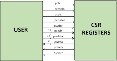
The APB signals will act as an interface to our system in which we can read/write the CSR registers. Here is the block diagram of our system:
Signals description:
pclk - Clock
presetn - Asynchronous reset
paddr - Address bus (12 bits)
pselx - Indicates slave is selected
penable - Indicates second and subsequent cycles of a transfer
pwrite - Indicates a write operation is taking place if high, else read
pwdata - Input data to be written (32 bits)
pready - Indicates successful read/write transfer completion
prdata - Output data that is read (32 bits)
Verilog Code Logic:
A state machine is designed with the following states: IDLE, SETUP, READ_STATE and WRITE_STATE.
- Initially, we are in IDLE state.
- As soon as pselx, paddr and pwrite becomes valid, we move to SETUP phase.
- Next cycle, penable occurs and we move to either READ_STATE or WRITE_STATE based on pwrite signal.
- In READ_STATE, we check paddr to see which CSR register is being accessed. Based on this, the data read is copied to prdata and ready signal pready is asserted.
- In WRITE_STATE, we check paddr to see which register is being written to. Based on this, pwdata is copied to the appropriate fields of the accessed register. Ready signal pready is asserted.
- When paddr falls out of range of any CSR register, we provide pslverr in this case.
Verilog Code:
module apb_csr(
	pclk,
	presetn,
	paddr,
	pselx,
	penable,
	pwrite,
	pwdata,
	pready,
	prdata,
	pslverr
    );

parameter ADDR_WIDTH = 12;
parameter DATA_WIDTH = 32;

//State machine states
parameter IDLE		= 2'b00;
parameter SETUP		= 2'b01;
parameter READ_STATE	= 2'b10;
parameter WRITE_STATE	= 2'b11;

//CSR Register addresses
parameter DATA_REG	= 12'h800;
parameter STATUS_REG	= 12'h804;
parameter INTERRUPT_REG	= 12'h808;

//APB Bus Signals
input pclk;
input presetn;
input [ADDR_WIDTH-1:0] paddr;
input pselx;
input penable;
input pwrite;
input [DATA_WIDTH-1:0] pwdata;

output reg pready;
output reg [DATA_WIDTH-1:0] prdata;
output reg pslverr;

reg [1:0] present_state, next_state;

reg next_pready;
reg [DATA_WIDTH-1:0] next_prdata;
reg next_pslverr;

//CSR Registers
reg [9:0] data1, next_data1;
reg [9:0] data2, next_data2;

reg overflow;
reg sign;
reg parity;
reg zero;

reg overflow_ie, next_overflow_ie;
reg sign_ie, next_sign_ie;
reg parity_ie, next_parity_ie;
reg zero_ie, next_zero_ie;


always @ (posedge pclk or negedge presetn) //Sequential Part
begin
  if (!presetn)
  begin
  pready	<= 1'b0;
  prdata	<= 32'h0;
  pslverr	<= 1'b0;

  data1		<= 10'd0;
  data2		<= 10'd0;
  overflow_ie	<= 1'b0;
  sign_ie	<= 1'b0;
  parity_ie	<= 1'b0;
  zero_ie	<= 1'b0;
  present_state <= IDLE;
  end

  else
  begin
  pready	 <= next_pready;
  prdata	 <= next_prdata;
  pslverr	 <= next_pslverr;

  data1		 <= next_data1;
  data2		 <= next_data2;
  overflow_ie	 <= next_overflow_ie;
  sign_ie	 <= next_sign_ie;
  parity_ie	 <= next_parity_ie;
  zero_ie	 <= next_zero_ie;
  present_state  <= next_state;
  end
end

always @ (*)  //Combinational Part
begin
  next_pready	 = pready;
  next_prdata	 = prdata;
  next_pslverr	 = pslverr;

  next_data1	 = data1;
  next_data2	 = data2;
  next_overflow_ie = overflow_ie;
  next_sign_ie	 = sign_ie;
  next_parity_ie = parity_ie;
  next_zero_ie	 = zero_ie;
  next_state	 = present_state;

  case(present_state)
  IDLE:
  begin
	 if(pselx)
	 next_state = SETUP;
	 else
	 next_state = present_state;
  end

  SETUP:
  begin
    if(penable && pwrite)
	 next_state = WRITE_STATE;
	 else if(penable)
	 next_state = READ_STATE;
	 else
	 next_state = present_state;

  end

  READ_STATE:
  begin
  	if(pready)
	begin
	next_state = IDLE;
	next_pready = 1'b0;
	end
	else
	begin
	next_pready = 1'b1;
		case(paddr)
		DATA_REG:
		  next_prdata = {12'b0, data1, data2}; //Read in the same order of fields

		STATUS_REG:
		  next_prdata = {28'b0, overflow, sign, parity, zero};

		INTERRUPT_REG:
		  next_prdata = {28'b0, overflow_ie, sign_ie, parity_ie, zero_ie};

		default:
		  next_pslverr = 1'b1;
		endcase
	end
	end

  WRITE_STATE:
  begin
  	if(pready)
	begin
	next_state = IDLE;
	next_pready = 1'b0;
	end
	else
	begin
	next_pready = 1'b1;
		case(paddr)

		DATA_REG:
		begin
		  next_data1 = pwdata[19:10]; //Write to appropriate bits
		  next_data2 = pwdata[9:0];
		end

		INTERRUPT_REG:
		begin
		  next_overflow_ie = pwdata[3];
		  next_sign_ie	   = pwdata[2];
		  next_parity_ie   = pwdata[1];
		  next_zero_ie	   = pwdata[0];
		end

		default:
		  next_pslverr = 1'b1;
		endcase
	end
	end
	endcase
end
endmodule
I have just given an example code with 3 registers. Like this, any number of registers can be added, using which we can perform read and write operations.
Thus, we have learnt:
1. Use of APB protocol to interface with CSR registers.
2. How to access CSR registers and perform read and write operations.

No comments:
Post a Comment