In this post, I will give a quick overview of the Xilinx Vivado Tool. It is a successor to the Xilinx ISE Tool and is used for FPGA design.
The complete design flow overview is given in the official documentation:
Vivado Design Flows Overview
This is a very extensive resource as this document links to many other documents that explain each process in great detail.
The complete design flow overview is given in the official documentation:
Vivado Design Flows Overview
This is a very extensive resource as this document links to many other documents that explain each process in great detail.
Vivado Tool Flow:
Basic Steps to follow at a Glance:
- Design entry using Verilog.
- Elaborate RTL to see raw schematic and ensure compliance to design rules.
- Write a testbench to perform behavioral simulation and observe the waveform.
- Netlist will be generated upon synthesis.
- Using netlist, a schematic representation is generated consisting of LUTs (combinational elements) and FDREs (FFs).
- You can add constraints such as mainly clock period, input delays and output delays. Perform I/O pin placement.
- Implementation performs Translate (the synthesized netlist), Map and Place-and-Route.
- After this, generate the bitstream to be loaded into hardware.
Let us have a more detailed look into each step.
(I have used a clock divider module)
Add the RTL files as a design source and the testbench as simulation sources in your Vivado project. Design entry is done here.
Ensure that top modules are selected correctly.

After elaboration, elaborate design option will directly present the schematic of the RTL.
What is elaboration?
The compiler explores the top-down design hierarchy and builds an interconnection table. The schematic consists of logic gates, MUX, registers etc.
 Also check Report Methodology and Report DRC to ensure that your design does not violate any design rules.
(I have used a clock divider module)
SOURCE FILES
Ensure that top modules are selected correctly.

ELABORATION
What is elaboration?
The compiler explores the top-down design hierarchy and builds an interconnection table. The schematic consists of logic gates, MUX, registers etc.


SIMULATION
Run behavioral simulation to directly simulate your HDL and see if the output is obtained as expected. In your testbench, give a reset time of 100 ns as it is the Global reset time for the FPGA.

Run Synthesis and correct all the errors/warnings present in the Messages tab of vivado.
See the schematic after Synthesis. Combinational elements are converted to Look-Up Tables (LUTs) and FDREs (Flip-flops). Also, buffers are added.

Synthesis report and utilization report is generated after synthesis.
The schematic generates the required cells (logic components) as shown above and the report provides the count of each.
Utilization report tells us how much of the resources are used from the available resources in the FPGA.

Like this, we have multiple tables that displays utilization for each kind of resource such as memory, DSP, IO, clocking etc.
After synthesis, we have two more types of simulation: functional and timing.
The basic difference between the three types:
After synthesis, we can invoke the constraints wizard to add certain design requirements called timing constraints.

SYNTHESIS
See the schematic after Synthesis. Combinational elements are converted to Look-Up Tables (LUTs) and FDREs (Flip-flops). Also, buffers are added.

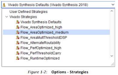
SYNTHESIS STRATEGIES
Incremental Synthesis: Synthesis will be re-run only on sections of design that have changed. Only from Vivado 2019.1 version.
Out-Of-Context Design Flow: Synthesis of modules independent from the hierarchy.
Synthesis and Implementation have to be re-run whenever a change is made in any design files.
SYNTHESIS REPORT
Synthesis report and utilization report is generated after synthesis.
The schematic generates the required cells (logic components) as shown above and the report provides the count of each.
Utilization report tells us how much of the resources are used from the available resources in the FPGA.
SIMULATION TYPES
The basic difference between the three types:
- Behavioral: Simulates the raw HDL code.
- Functional: Tests the logic "functional" operation of the circuit after synthesis or implementation but no delays are considered.
- Timing: Delay through the internal logic or the routing delay paths associated with where the placer and the router interconnect things is considered.
TIMING CONSTRAINTS
- What is it? A series of constraints applied to a given set of paths or nets that dictate the desired performance of a design. Constraints may be period, frequency, net skew, maximum delay between end points, or maximum net delay. Basically there are two types: Physical constraints and timing constraints.
- Why we need it? Timing constraints may be used to influence and guide the placement of design elements and signal routes between placed elements in order to meet design performance requirements.
- In Vivado: Using constraint wizard, we can constrain clocks, input and output delays, CDC etc .

On opening the constraints wizard, it will ask you to create a new constraints file into the project and set it as target. After this, re-synthesize and run the Constraints wizard again.
- First create a clock with the desired frequency.
- To complete implementation without error, this is enough. But it is recommended to add all possible constraints for best implementation of the design.
PIN PLACEMENT

In Synthesized Design window, Right click on package window and tile vertically.
Under Package Pins Tab, you can select a I/O Bank. It will be highlighted on the package as well as device.
Package means just I/O ports view, Device will show the internal structure as well.

Now we have to place the pins on the FPGA.
Place the desired pins on your ports from the I/O ports Tab.
If you want the tool to automatically do this for you,
Goto Tools -> I/O Plannning -> Autoplace I/O Ports
However, Auto placement can give you a critical warning saying that wrong placement can damage your device, it is recommended that users place it themselves.
Now you can run implementation to implement the design.
It consists of the following steps:
Translate:
Here the previously generated netlist is utilized and the ports are assigned to the physical elements like pins, switches in the design.
Map:
We know that the FPGA consists of Configurable Logic blocks and I/O blocks. The mapping process divides a design into sub blocks to fit into these FPGA blocks.
Place and Route:
In the final step, the different blocks are interconnected together in an optimum way to complete the design.
The final design is called the Implemented Design.
After running implementation, Press Ctrl + A on Netlist Tab to view the logic blocks that have been used up by your design on the device.

After implementation, Report Timing Summary is an important Report that details the complete timing analysis of the design (whether the required timing constraints have been met)
Open it from the Reports menu for detailed report.
Even though timing analysis can be performed after synthesis, the most accurate timing estimates comes only after running implementation.
Open it from the Reports menu for detailed report.
Even though timing analysis can be performed after synthesis, the most accurate timing estimates comes only after running implementation.
Always ensure that the slack value is positive in the timing reports to meet timing.
Refer to the Xilinx documentation for detailed information:
Design Analysis and Closure Techniques
Other resources on timing analysis:
FPGA Timing
Meaning of set_input_delay and set_output_delay in SDC timing constraints
Refer to the Xilinx documentation for detailed information:
Design Analysis and Closure Techniques
Other resources on timing analysis:
FPGA Timing
Meaning of set_input_delay and set_output_delay in SDC timing constraints
No comments:
Post a Comment