The previous two sections of the Processor Design series explored the intricacies involved in designing a simple MIPS based processor. In this final section, we will look at how the processor can be simulated and how we can check the results.
In Part 1 of the series, we had loaded three memories namely, the Instruction Memory, the Register file contents and the Data Memory using respective mem files.
Let us see how to provide data to the mem files to simulate the processor.
Instruction Memory (instrn_memory.mem)
Consider the following assembly code that you want to simulate using this processor.
(The number on the left represents instruction address)
00: add $t1, $t2, $t3
04: lw $t1, $t2, 16'd4
08: beq $t1, $t2, offset
0C: add $t1, $t2, $t3
10: or $t2, $t3, $t4
14: sw $t1, $t2, offset
Totally we have 6 instructions. Now let us write them in the number code format based on the type of instruction (R or I-Type) as we discussed earlier.
The code for each MIPS instruction is taken from the MIPS instruction manual and for the registers, it is taken from the register table as mentioned earlier.
So the code now becomes:
00: 6'd0,5'd9,5'd10,5'd11,5'd0,6'h20
04: 6'h23,5'd9,5'd10,16'd4
08: 6'h04,5'd9,5'd9,16'd1
0C: 6'd0,5'd9,5'd10,5'd11,5'd0,6'h20
10: 6'd0,5'd10,5'd11,5'd12,5'd0,6'h25
14: 6'h2B,5'd9,5'd10,16'd4
Convert this to hexadecimal representation:
00: 01 2A 58 20
04: 8D 2A 00 04
08: 11 29 00 01
0C: 01 2A 58 20
10: 01 4B 60 25
14: AD 2A 00 04
This is the data that we need to load in the instruction memory in a byte-wise manner.

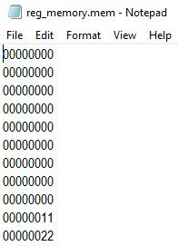
Register Memory (reg_memory.mem)
This is the memory where the memory location corresponds to the particular register address.
We are using the following registers $t1, $t2, $t3 and $t4 in our above code which corresponds to the register addresses 09, 10, 11 and 12.
Let us write some initial data 11 in $t1 and 22 in $t2. (locations 09 and 10)
Then the reg_memory.mem will look like this:
Data Memory (data_memory.mem)
As we know, this memory is used during the load and store operations. Let us fill some initial values in the memory as well.

Testbench:
Now we are completely ready with the Verilog design files for this simple processor.
The testbench for this will be simple. We just have to provide the clock and reset. The instruction memory will be loaded with the desired instructions and the simulation will take place as intended.
Here is the testbench to simulate the processor:
module Processor_Top_tb;

// Inputs
reg clk;
reg rst_n;

// Instantiate the Unit Under Test (UUT)
Processor_Top uut (
	.clk(clk),
	.rst_n(rst_n)
);

always #5 clk = ~clk;

initial begin
	clk = 1'b1;
	rst_n = 1'b0;
	#30
	rst_n = 1'b1;
	#70
	$finish;
end

endmodule


I agree it is not the easiest of waveforms to comprehend at a glance!
out_address shows the present address 00h.
No comments:
Post a Comment