FPGA (Field Programmable Array) consists of the following: Reprogrammable Logic Blocks, Programmable Interconnects and I/O blocks. Let us look at how timing analysis can be performed using Xilinx Vivado Tool.
FPGA Logic
Basically, FPGA logic comprises of:
1. Look-Up Tables (LUT): These are much like truth tables: all possible combinations of the inputs are tried and an output logical expression is obtained.
2. FDREs: These are the primitive D-type flip flops in Virtex FPGAs
3. RAM: The RAM memory in FPGA can either be Distributed RAM or Block RAM. Distributed RAM is used for small memories that can be distributed around different parts of the FPGA to improve access speeds. Block RAM is a single block of memory typically suitable for large sized memories.
4. DSPs: Digital Signal Processing blocks are dedicated blocks present in the FPGA to perform certain complex calculations.
The design must efficiently utilize the available reseources on the FPGA according to the provided constraints.
Basics of Static Timing Analysis
Basically, we have to ensure that the Setup times and Hold times of all the Flip-flops present in the design are satisfied.
Two types of analysis are performed: Setup analysis and Hold analysis
During Setup Analysis
Data arrival time = Propagation delay of flip-flop + combinational delay
Data required time = time duration of clock cycle + skew – setup time of FF
Slack = Data required time - Data arrival time
During setup time analysis, consider the maximum data path delays and minimum delays in the clock path
During Hold Analysis
Data arrival time (to next FF) = Propagation delay of flip-flop + combinational delay
Data required time = hold time of current FF
Slack = Data arrival time - Data required time
During hold analysis, consider minimum delays in the data path and maximum delays in the clock path
The difference in between data required time and data arrival time is called as slack and to meet setup/hold time the slack should be positive according to the appropriate formula.
Sometimes, hold time can be negative. Negative hold time (eg. -2ns) means the input can change 2ns before the clock edge, still the earlier input will be latched. So, it is not wrong to have a negative hold time.
So due to the above reasons, the higher we increase the clock frequency, the design timing issues will tend to increase. In simple terms, when I say my design works upto a clock frequency of 100 MHz (10 ns), it essentially means that data is able to propagate between any two adjacent clocked elements (flip-flops) within 10 ns (best case). So it is clear that as we increase clock frequency, we are reducing the time given for data propagation.
How do we find the maximum clock frequency at which the design can operate?
Maximum operating frequency is obtained when Required Time = Arrival Time
For any RTL design there can be four types of timing paths where min/max delays have to be analyzed and they are named as
- Input-to-register path (Input-to-reg path)
- Output-to-register path (output-to-reg path)
- Register-to-register path (Reg-to-reg path)
- Input-to-output path (combinational path)
Note: Path Delay = Cell Delay (Input transitions / Fanout loads) + Net Delay (Wire load models)
The path between the input and output that causes the maximum delay is called the Critical Path and these paths become the major obstacle to achieving Timing Closure.
FPGA Timing Analysis
Create constraints: 4 Key steps
- Create clocks
- Define clocks interactions
- Set input and output delays (board architecture knowledge will be helpful)
- Set timing exceptions
Handling CDC (Clock Interactions)
Xilinx Vivado reports unsafe CDC paths when the source and destination clocks do not share a common primary clock. This does not mean that the path is actually unsafe, it means that Vivado is not able to come to a conclusion about the path safety, and it has to be taken care by the user.
Tcl command:
set_clock_groups -asynchronous -group [get_clocks(clock1 )] -group [get_clocks(clock2)]
This constraint will tell Vivado not to consider timing analysis between clock1 and clock2 because the user has already taken care of CDC considerations between the two clocks.
There are also two more options namely:
- set_false_path: Just like set_clock_groups, this also informs Vivado that paths under this label need not be considered for timing analysis. But set_clock_groups is easier to use as more inputs can be considered easily for exemption.
- set_multicycle_path: This explicitly informs the tool that the paths under this label require more than a single clock cycle to execute.
How to take care of CDC?
I won't explain in detail but here are some quick points to keep in mind:
- Slow to fast clock crossing - Double flop synchronizer will suffice
- Fast to slow clock crossing - Requires feedback / mux-based synchronizer or even asynchronous FIFO
- Reconvergence issue or multi-bit data loss. When multi-bit data needs to be synchronized, we only synchronize the control signals, based on that multi-bit data can be transferred.
Constraints Wizard
In order to ease the process of constraints creation, Xilinx Vivado Tool features a constraints wizard that walks you through various timing constraints that can be set.
Reports Checking and Debugging
After the synthesis or implementation stage, the following Tcl commands can be used to check various timing reports.
- report_timing_summary
- check_timing
- report_clocks
- report_clock_networks
- report_clock_interaction
- report_timing
The slack value is calculated for setup analysis as well as hold analysis. In order to pass timing checks, the slack must be positive across all timing paths.
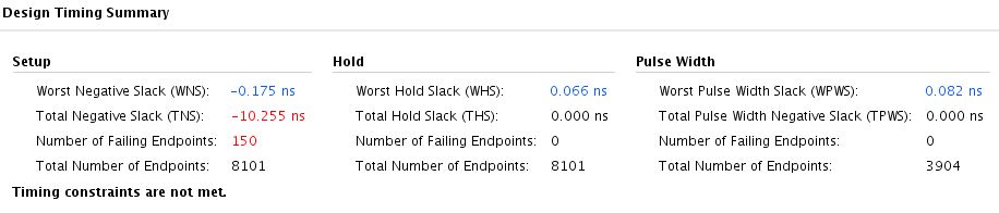
Sample Timing Report showing Setup slack violations
FPGA Timing Closure
Timing Closure is defined as the condition that arises when all paths in the design have passed timing checks and all slack is positive.
Achieving FPGA timing closure requires a lot of testing and iteration steps in the implementation phase. The timing report can be reviewed after synthesis itself, to get an idea of approximate timing. Synthesis tools use loading model to estimate delays which can be a bit pessimistic, but they give an idea of the timing range you can expect. The exact values can be viewed after the implementation step.
Here are some of the quick tips that can be followed to tread the path of achieving timing closure:
Design Constraints check
Firstly check your design constraints to ensure that the design is not so unreasonably constrained that timing closure achievement is near impossible. In such cases, it is advised to relax certain constraints for better design performance.
Most importantly, the clock frequency of the design must be set at a reasonable value.
Delay Optimization
Check the timing report to see which type of delay is the major contributor to timing failure. There are two options:
- Logic Delay: If large combinational logic is used, then the delay across the logic itself can cause timing failure.
- Net Delay: Usually, net delay dominates the timing path delay, which is a measure of how the nets are routed across the design.
If the logic delay is contributing significantly to the path delay, try to reduce the number of logic levels.
Number of logic levels is calculated by the formula:
Clk to out of a CLB Register + LUT Delay + Setup time of CLB Register
Reduction in logic levels is most easily achieved by good HDL design practice.
If some nets are highly loaded (high fanout), the delay will be more and it can be reduced by logic replication, meaning the logic output net fanout is reduced with each replicated logic.
If you want to limit the net fanout, use set_max_fanout command.
Pipelining combinational logic is another useful technique to reduce latency. If a combinational path is too long, then registers can be placed at intermediate regions.
This will serve the dual purpose of reducing the latencty, as well as providing a pipelined operation that reduces the overall clock cycles to provide the output.
Now assume net delay is the major contributor of path delay. Net delay will be large in cases where routing paths are long. This usually happens when signals are routed between different design modules with only combinational logic.
The best way of solving this issue is to register the inputs at the destination module which are part of a critical path (meaning adding a flip-flop).
This will help to cut off the critical path length at the input of the destination module and in turn, reduce the net delay.
Apart from these HDL coding methods of reducing timing delays, there are many other optimizations that can be done at the placement stage which we shall not cover here.
The Xilinx Vivado tool offers many synthesis and implementation strategies which take special care in performing certain optimization such as area, power or timing optimization. Using a timing optimized strategy will also be a significant step taken towards achieving timing closure.
References:
No comments:
Post a Comment